Categories
Tags
-
#SEO
#One-Color Closed Ink Cup Pad Printer
#Carbide Ring for Pad Printing Ink Cups
#Motocross Goggles
#At GAIA
#we specialize in the field of flexible packaging
#offering a wide range of innovative and high-quality packaging solutions.
#custom CNC milling services
#Ceramic Lamp Holder
#Wire Electric Motor Automatic Coil Winding Machine
#skiing helmets
#Ground Coffee Bags
#Four Color Pad Printing Machine
#Precision stamping
#Deep drawing
#丝印机
#Ben Wa Balls for Women
#Cantilever Single Twisting Machine
#fashion boxes and bags
#rigid-flex PCBs
#sealed ink cups
#ski goggles
Archives
The Unsung Heroes: Mars PCB and the Future of Integrated Circui
-
Posted by TTTTT KKKKK - Filed in Arts & Culture - 647 views
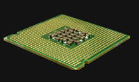
The global integrated circuit (IC) shortage of 2020-2022 served as a stark reminder of the foundational role that ICs play in virtually every electronic device we use today. Yet, the performance of these tiny silicon wonders is only as good as their connection to the wider world. This critical link is provided by specialized integrated circuit substrates—a type of advanced PCB designed to package and support the IC, ensuring a strong, reliable connection to the primary circuit board. Mars PCB stands at the forefront of this crucial technology, providing expert PCB assembly services that are essential for the creation of high-quality IC substrates, thereby guaranteeing optimal performance for your electronic products.
An IC substrate is far more than a simple carrier; it is a sophisticated, multi-layered board that provides electrical connections, thermal dissipation, and mechanical support for the IC. It acts as the bridge between the microscopic world of the silicon die and the macro world of the main PCB, a role that demands exceptional precision and reliability. As ICs become smaller, more complex, and faster, the demands on their substrates have grown exponentially.
Understanding these demands requires an exploration of the manufacturing processes behind IC substrates. Traditionally, these boards were produced using subtractive methods, where a copper-clad laminate is etched to remove unwanted material, leaving behind the desired circuit traces. While effective for less dense designs, this method has limitations in creating the ultra-fine lines and spaces required for today’s high-density ICs.
The evolution of technology has led to the development of more advanced techniques, most notably the semi-additive method (SAP). This process begins with a very thin layer of copper, onto which a pattern is applied. The circuit traces are then built up, or "added," to this pattern using an electroless and electrolytic plating process. This revolutionary approach allows for significantly finer lines and spaces, enabling the creation of substrates with much higher density and more complex routing. SAP is the key to packaging the most advanced ICs, facilitating greater functionality and miniaturization in a wide array of devices.
At Mars PCB, we leverage this evolution in manufacturing, offering a comprehensive understanding of IC substrates from their definition and applications to the intricate processes that bring them to life. By focusing on advanced manufacturing techniques, we ensure that the substrates we produce are perfectly suited for today’s high-performance ICs. Our expert assembly services guarantee that every IC is mounted with the precision required for seamless integration and long-term reliability, positioning Mars PCB as your trusted partner in building the future of electronics.